

Wet chemical techniques have been used to produce a wide variety of metal and semiconductor nanocrystals, including Au and Ag nanocrystals, with fascinating plasmonic properties in the visible to near infrared region.
Photo credit: Macro Photo / Shutterstock.com
The latest study published in ACS Omega focuses on WO3-Au hybrids and their efficient properties.
Properties of WO3-Au metal / semiconductor hybrid
A simple hydrothermal approach was used to create a WO3-Au metal / semiconductor hybrid that consisted of a backbone of WO3 nano-building blocks that were reinforced by the presence of Au-nano-particle additives. The WO3-Au hybrids offer superior light absorption, robust plasmonic interaction, superior performance SERS, and catalytic properties.
In addition, the WO3-Au hybrids show remarkable photocatalytic properties for RhB degradation when irradiated with visible light. The robust plasmonic resonance and the effective conduction mechanism between Au and WO3 nanocomponents are attributed to the increased photocatalytic performance. This study would prove particularly fruitful for the electronics sector and all other structural industries that use semiconductor-metal hybrids.
Industrial use
Such metal-semiconductor hybrids have found their application in many industries, from high-tech industrial applications on the macro scale to technological applications on the nano scale. The most important are plasmonic applications. These include plasmonic catalytic reactions, the photogeneration of pollutants, the photocatalytic hydrogen synthesis and the photocatalytic CO2 process.
Optical applications are also an important area, including plasmon enhanced photoluminescence and surface enhanced Raman applications. Solar cell applications and biotechnological applications also use this advantageous substance for their applications without further ado.
limitations
While many of its advantages are known, some limitations also act as a hurdle to its rapid commercialization and wide-ranging applications. Due to the Lar-Mer growth process of the high-temperature synthesis of organic phases, the metal or semiconductor component could not be in larger dimensions, such as. B. a few tens to hundreds of nanometers.
Another big problem is the size of the two components; since it is still mainly limited to the 10 nm range, the transition between metal and semiconductor is not yet kept sufficiently clean.
Materials and methods
The materials used in this experiment included ninety nine point five percent sodium tungstate (99.5%), ninety nine point seven percent L-ascorbic acid, hydrochloric acid (30%), and chloroauric acid (99.9%).
The first step was the synthesis of the semiconductor hybrid. A simple hydrothermal process was used to make the WO3 nanostones. A reactor was charged with 20 ml of sodium tungstate (0.01 M) and 6 ml of chloroauric acid. The mixed solution was placed on a hot plate and heated at 180 ° C. for 24 hours. In order to eliminate impurities, the finished products were centrifuged at 5000 rpm for 5 minutes.
For SERS measurements, RhB molecules were placed as substrates on WO3 and WO3-Au hybrids. The substrates were prepared by combining 1 ml of RhB in various concentrations with 0.5 ml of WO3 and WO3-Au (0.5 mg ml1). The solution was mixed and left in the dark for 2 hours.
The photocatalytic abilities of WO3 and WO3-Au hybrids were assessed using RhB photodegradation under the illumination of a 300 W xenon lamp with an ultraviolet exclusion filter.
The TEM images were recorded with a JEOL 2100 at 200 kV. HRTEM and EDS were performed using a JEOL 2010 FET microscope with a 200 kV accelerating voltage.
Experimental results
The experimental results confirmed that the WO3 had a flat surface and a consistent brick shape. The growth of Au nanoparticles on WO3 nanostones led to Au-decorated WO3 nanostones, with chloroauric acid and ascorbic acid serving as precursors and reducing agents, respectively.
The research showed that the Au nanoparticles have a flower-like shape with an average size of 34 nm. With a grid spacing of 0.38 nm, the WO3 nanostone exhibited continuous and ordered grid fringes. The WO3 pattern corresponded well to the triclinic phase of WO3. The topology of the WO3 Au semiconductor / metal hybrids was modified by varying the amount of chloroauric acid used during the manufacturing process.
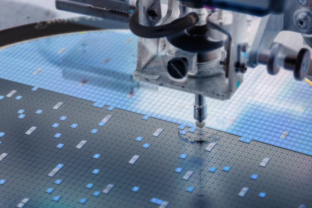
Image source: Mike_shots / Shutterstock.com
The flexural vibration mode of OWO was held responsible for the conspicuous peaks at 275 and 328 cm-1. The peaks at 712 and 810 cm-1 are caused by the stretching mode of WO. The oxygen vacancies on the surface of WO3 can provide additional active sites for the adsorption of RhB.
The Raman amplitude of the WO3-Au hybrids at 1647 cm1 was corresponding to 1.98 and 5.86 times that of Au nanoparticles and WO3. The Raman intensity of WO3-Au (2.1% by weight) at 1647 cm1 was 10.4 and 3.51 times that of pure WO3 and Au nanoparticles, respectively. The minimum measurable limit is 10-12 M, while the highest EF (at 1647 cm-1) is determined to be 5.3 * 108.
Additional Au nanoparticles can be added to increase the number of interlayer hotspots. The more Au nanoparticles are placed on WO3 nanostones, the larger and stronger the electromagnetic hotspots induced by plasmon coupling, which equip WO3-Au (2.1% by weight) with excellent SERS sensitivity.
The plasmonic resonance of Au nanoparticles can be stimulated by visible light, which can increase the light-gathering capacity of the WO3-Au hybrids. In addition, the activation process between Au and WO3 can accelerate carrier separation and improve photocatalytic activity and efficiency.
The study found that the photocatalytic activity of WO3-Au (2.9 wt%) is lower than that of WO3-Au (2.1 wt%). Excess Au nanoparticles on WO3 can act as recombination centers, slowing down the charge transfer and thus reducing the photocatalytic effectiveness.
limitations
Although the study carefully examined the semiconductor hybrid, its results still have one caveat. These results are only applicable to semiconductors made from a WO3-Au mixture. The values cannot be generalized for all hybrid semiconductors. Therefore, new experiments and findings are essential for other semiconductors.
In short, research has thoroughly examined almost all of the essential aspects of the specific type of semiconductor hybrids. The results would increase their efficiency significantly, resulting in massive lifespan extensions, lower operating costs, and massive growth in rapid commercialization.
References
Tang, L., Liang, S., Li, JB, Zhang, D., Chen, WB, Yang, ZJ,. . . Wang, QQ (2020). Controlled synthesis of Au nanocrystals-metal-selenide hybrid nanostructures for a plasmon-enhanced photoelectrochemical energy conversion. Nanomaterials. https://www.mdpi.com/2079-4991/10/3/564
Volokh, M., & Mokari, T. (2020). Metal / semiconductor interfaces in nanoscale objects: synthesis, new properties and applications of hybrid nanostructures. Advances in the Nanoscale, 930-961. https://pubs.rsc.org/en/content/articlelanding/2020/na/c9na00729f
Zhang, J., Ji, M., Liu, J. & Xu, M. (2016). Metal / semiconductor hybrid nanocrystals and synergistic photocatalysis applications. Advanced Catalytic Materials – Photocatalysis and Other Current Trends. https://www.intechopen.com/chapters/49640
Zou, JW, Li, ZD, Kang, HS, Zhao, WQ, Liu, JC, Chen, YL,. . . Ding, SJ (2021). Strong absorption of visible light and numerous hotspots in Au-decorated WO3 nanobricks for efficient SERS and photocatalysis. ACS-Omega, 28347-28355. https://pubs.acs.org/doi/10.1021/acsomega.1c04536
Disclaimer: The views expressed here are those of the author in his private capacity and do not necessarily reflect the views of AZoM.com Limited T / A AZoNetwork, the owner and operator of this website. This disclaimer is part of the terms of use for this website.
Comments are closed.